д»ӘеҷЁд»Ӣз»Қ
Anasysзҡ„nanoIR2sзі»з»ҹжҳҜеёӮеңәдёҠе”ҜдёҖдёҖж¬ҫеҗҢж—¶е…·еӨҮзәізұіе°әеәҰзәўеӨ–еҗёж”¶е…үи°ұжөӢиҜ•пјҲAFM-IRпјүе’Ңж•Је°„ејҸиҝ‘еңәжҲҗеғҸ(s-SNOM)еҠҹиғҪзҡ„и®ҫеӨҮгҖӮAFM-IRеҠҹиғҪйҮҮз”Ёдё“еҲ©еҢ–зҡ„е…үзғӯиҜұеҜје…ұжҢҜжҠҖжңҜпјҲPTIRпјүеҲӣйҖ жҖ§зҡ„дҪҝз”ЁAFMжҺўй’ҲдҪңдёәеҫ®еҢәзәўеӨ–еҗёж”¶зҡ„дј ж„ҹеҷЁпјҢе…үи°ұзҡ„з©әй—ҙеҲҶиҫЁзҺҮдёҚеҶҚдҫқиө–е…үж–‘иҒҡз„Ұе°әеҜёпјҢз©әй—ҙеҲҶиҫЁзҺҮдјҳдәҺ100nmз©әй—ҙеҲҶиҫЁзҺҮгҖӮsSNOMеҠҹиғҪйҮҮз”Ёдё“еҲ©и®ҫи®Ўзҡ„жҢҜе№…и°ғеҲ¶жҠҖжңҜпјҢиҺ·еҫ—иҝ‘еңәдҝЎеҸ·ејәеәҰе’ҢзӣёдҪҚзҡ„еҗҢжӯҘжҲҗеғҸпјҢжңҖдҪіз©әй—ҙеҲҶиҫЁзҺҮеҸҜиҫҫ10nmгҖӮ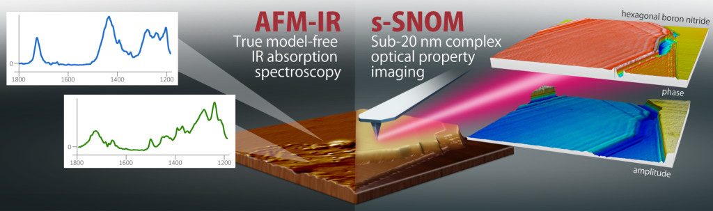
дә§е“Ғзү№зӮ№
-
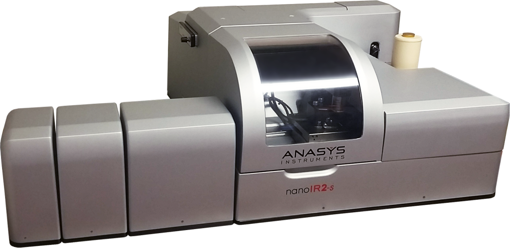
nanoIR2-s
-
зәізұізәўеӨ–еҗёж”¶е…үи°ұ + ж•Је°„ејҸиҝ‘еңәжҳҫеҫ®й•ң
AFM + sSNOM
иҜҘзі»з»ҹдё»иҰҒеҢ…жӢ¬ж•Је°„ејҸиҝ‘еңәжҳҫеҫ®й•ңжЁЎеқ—пјҲsSNOMпјүпјҢзәізұізәўеӨ–еҗёж”¶жЈҖжөӢжЁЎеқ—пјҲAFM-IRпјүе’ҢеҺҹеӯҗеҠӣжҳҫеҫ®й•ңжЁЎеқ—пјҲAFMпјүгҖӮ
еҮ дёӘжЁЎеқ—зҡ„дё»иҰҒзү№зӮ№пјҡ
|
|
ж•Је°„ејҸиҝ‘еңәжҳҫеҫ®й•ңжЁЎеқ—пјҲsSNOMпјү
|
зәізұізәўеӨ–еҗёж”¶жЈҖжөӢжЁЎеқ—пјҲAFM-IRпјү
|
еҺҹеӯҗеҠӣжҳҫеҫ®й•ңжЁЎеқ—пјҲAFMпјү
|
|
жЈҖжөӢеҺҹзҗҶ
|
1. жЈҖжөӢж•Је°„е…үпјӣ
2. жҸҗдҫӣе…ү-зү©иҙЁзӣёдә’дҪңз”ЁжҲҗеғҸе’Ңе…үи°ұпјӣ
|
1. жЈҖжөӢе®ҳиғҪеӣўжҢҜеҠЁеҗёж”¶дә§з”ҹзҡ„зғӯиҶЁиғҖдҝЎеҸ·пјӣ
2. жҸҗдҫӣзңҹе®һзҡ„зәўеӨ–еҗёж”¶е…үи°ұе’ҢжҲҗеғҸ.
|
е·ҘдҪңжЁЎејҸпјҡжҺҘи§ҰгҖҒиҪ»ж•ІгҖҒзӣёдҪҚгҖҒеҠӣжӣІзәҝгҖҒеҠӣи°ғеҲ¶гҖҒжЁӘеҗ‘еҠӣгҖҒеҠ зғӯжҺўй’ҲеҺҹеӯҗеҠӣжҳҫеҫ®й•ңгҖҒе…¶д»–жЁЎејҸеҸҜеўһеҠ пјӣ
|
|
дё»иҰҒеә”з”Ё
|
иЎЁйқўзӯүзҰ»еӯҗдҪ“гҖҒзәізұіеӨ©зәҝгҖҒ2Dжқҗж–ҷпјҲзҹіеўЁзғҜпјҢBNпјүпјҢзәізұіз»“жһ„пјҢеҚҠеҜјдҪ“пјҢз»қзјҳдҪ“пјҢз”ҹе‘Ҫ科еӯҰпјҢй«ҳеҲҶеӯҗжқҗж–ҷзӯү
|
иЎЁйқў/з•ҢйқўеҲҶжһҗпјҢеӨҡзӣёеӨҚеҗҲз»“жһ„пјҢеӨҡеұӮиҶңз»“жһ„пјҢе°Өе…¶йҖӮз”ЁдәҺе…·жңүдёҖе®ҡзғӯиҶЁиғҖзі»ж•°зҡ„иҪҜиҙЁжқҗж–ҷпјҢеҰӮпјҡй«ҳеҲҶеӯҗпјҢеӨҚеҗҲжқҗж–ҷгҖҒз”ҹе‘Ҫ科еӯҰзӯү
|
еҗ„з§ҚжңүжңәгҖҒж— жңәгҖҒеҚҠеҜјдҪ“гҖҒз»қзјҳдҪ“гҖҒзәізұіжқҗж–ҷгҖҒз”ҹе‘Ҫ科еӯҰзӯү
|
дёҖгҖҒs-SNOMж•Је°„ејҸиҝ‘еңәе…үеӯҰжҳҫеҫ®й•ң
ж•Је°„ејҸиҝ‘еңәе…үеӯҰжҳҫеҫ®й•ңпјҲs-SNOMпјүжҳҜдёҖз§Қе…Ҳиҝӣзҡ„иҝ‘еңәе…үеӯҰжҠҖжңҜпјҢдҪҝз”ЁйҮ‘еұһй•ҖеұӮAFMжҺўй’Ҳд»Јжӣҝдј з»ҹе…үзәӨжҺўй’ҲжқҘеўһејәе’Ңж•Је°„ж ·е“ҒзәізұіеҢәеҹҹеҶ…зҡ„е…үиҫҗе°„пјҢд»ҺиҖҢиҺ·еҫ—жӣҙй«ҳзҡ„з©әй—ҙеҲҶиҫЁзҺҮгҖӮз”ұдәҺs-SNOMйҮҮз”ЁAFMй’Ҳе°–дҪңдёәж•Је°„жәҗпјҢиҝ‘еңәе…үеӯҰзҡ„еҲҶиҫЁзҺҮд»…з”ұAFMй’Ҳе°–зҡ„жӣІзҺҮеҚҠеҫ„еҶіе®ҡпјҢдёҺе…Ҙе°„е…үжәҗзҡ„жіўй•ҝж— е…іпјҢs-SNOMзҡ„з©әй—ҙеҲҶиҫЁзҺҮеҸҜиҫҫ20nmпјҲжңҖдҪіеҸҜиҫҫ10nmпјүгҖӮs-SNOMе№ҝжіӣйҖӮз”ЁдәҺж— жңәзү©е’Ңжңүжңәзү©пјҢе°Өе…¶жҳҜе…·жңүй«ҳеҸҚе°„зҺҮпјҢй«ҳд»Ӣз”өеёёж•°е’Ңејәе…үеӯҰе…ұжҢҜзҡ„жқҗж–ҷгҖӮ
-
10nmз©әй—ҙеҲҶиҫЁзҺҮиҝ‘еңәжҲҗеғҸе’Ңе…үи°ұ
-
зӢ¬жңүеҝ«йҖҹжҲҗеғҸе’ҢйҮҮи°ұжҠҖжңҜпјҢ10еҖҚдәҺдј з»ҹspatio-spectral imaging
-
дё“еҲ©иғҢжҷҜеҺӢеҲ¶жҠҖжңҜе’Ңй«ҳж•Ҳе…үеӯҰдҝЎеҸ·ж”¶йӣҶжҠҖжңҜпјҢзЎ®дҝқй«ҳдҝЎеҷӘжҜ”
-
йў„е…Ҳж ЎеҮҶе…үи·ҜпјҢж“ҚдҪңжһҒе…¶з®Җдҫҝ
-
жЁЎеқ—еҢ–и®ҫи®ЎпјҢеҸҜжӢ“еұ•жҖ§ејә
-
зӯүзҰ»жҝҖе…ғзҡ„й«ҳеҲҶиҫЁзҺҮжҲҗеғҸе’ҢеҲҶжһҗ
-
е№ҝжіӣйҖӮз”ЁдәҺеҗ„з§Қж— жңәзү©е’Ңжңүжңәзү©
дәҢгҖҒAFM-IRзәізұізәўеӨ–е…үи°ұ
AFM-IRжҠҖжңҜжҳҜзҫҺеӣҪAnasysд»ӘеҷЁе…¬еҸёз ”еҸ‘зҡ„дёҖж¬ҫеҹәдәҺеҺҹеӯҗеҠӣжҳҫеҫ®й•ңпјҲAFMпјүзҡ„жқҗж–ҷиЎЁеҫҒжҠҖжңҜпјҢд№ҹжҳҜеёӮйқўдёҠе”ҜдёҖеҸҜд»ҘзӣҙжҺҘжҺўжөӢзәізұіе°әеҜёзәўеӨ–еҗёж”¶е…үи°ұзҡ„е…ҲиҝӣжҠҖжңҜгҖӮAFM-IRйҮҮз”ЁеҠҹиғҪејәеӨ§зҡ„е…үзғӯиҜұеҜје…ұжҢҜжҠҖжңҜпјҲPTIRпјүпјҢдҪҝзәўеӨ–е…үи°ұзҡ„з©әй—ҙеҲҶиҫЁзҺҮзӘҒз ҙдәҶе…үеӯҰиЎҚе°„жһҒйҷҗпјҢжҸҗй«ҳиҮі100nmд»ҘдёӢпјҢеё®еҠ©з ”究дәәе‘ҳжӣҙе…Ёйқўең°дәҶи§Јзәізұіе°әеәҰдёӢж ·е“ҒиЎЁйқўеҫ®е°ҸеҢәеҹҹзҡ„еҢ–еӯҰдҝЎжҒҜгҖӮз”ұдәҺе…¶е®һзҺ°дәҶи¶…й«ҳз©әй—ҙеҲҶиҫЁзҺҮзҡ„зәўеӨ–е…үи°ұйҮҮйӣҶпјҢиҜҘжҠҖжңҜжӣҫиҚЈиҺ·2010е№ҙеәҰзҫҺеӣҪR&D100еӨ§еҘ–гҖӮ
з”ұдәҺдј з»ҹзҡ„зәўеӨ–е…үи°ұжҠҖжңҜйңҖиҰҒйҮҮйӣҶзәўеӨ–е…үйҖҸиҝҮж ·е“ҒпјҢжҲ–еңЁж ·е“ҒиЎЁйқўеҸҚе°„зҡ„е…үдҝЎеҸ·пјҢеӣ жӯӨеңЁжЈҖжөӢеҫ®е°ҸеҢәеҹҹж—¶еҝ…然еҸ—еҲ°е…үеӯҰиЎҚе°„жһҒйҷҗзҡ„йҷҗеҲ¶пјҢдҫӢеҰӮеӮ…з«ӢеҸ¶зәўеӨ–е…үи°ұпјҲFTIRпјүзҡ„з©әй—ҙеҲҶиҫЁзҺҮеҸӘжңү10пҪһ30 ОјmпјҢе…ЁеҸҚе°„иЎ°еҮҸзәўеӨ–е…үи°ұпјҲATR-IRпјүзҡ„з©әй—ҙеҲҶиҫЁзҺҮеҸӘжңү3пҪһ5 ОјmпјҢйҡҫд»Ҙж»Ўи¶ізәізұіе°әеәҰдёӢзҡ„жЈҖжөӢдёҺиЎЁеҫҒйңҖиҰҒгҖӮ
зҫҺеӣҪAnasysд»ӘеҷЁе…¬еҸёзҡ„第дәҢд»ЈзәізұізәўеӨ–е…үи°ұд»ӘеҲӣйҖ жҖ§ең°дҪҝз”ЁAFMжҺўй’Ҳй’Ҳе°–жқҘжЈҖжөӢж ·е“Ғзҡ„зәўеӨ–еҗёж”¶дҝЎеҸ·пјҢд»ҺиҖҢе®һзҺ°дәҶз©әй—ҙеҲҶиҫЁзҺҮдҪҺдәҺе…үеӯҰиЎҚе°„жһҒйҷҗзҡ„зәўеӨ–е…үи°ұеҲҶжһҗгҖӮ
жҠҖжңҜеҸӮж•°
hBN еЈ°еӯҗжһҒеҢ–жҝҖе…ғ
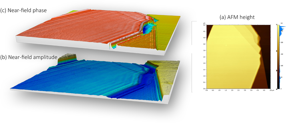
Nano imaging of surface phonon polaritons (SPhP) on hexagonal boron nitride (hBN). (a) AFM height image shows homogeneous hBN surface with different layers on Si substrate; (b) s-SNOM amplitude shows strong interference fringes due to propagating SPhP along the surface on hBN; (c) s-SNOM phase shows a difference phase with layer thickness. From the image b and c, we can also see the wavelength of the SPhP changes with the number of layers.
зҹіеўЁзғҜеҹәзӯүзҰ»еӯҗдҪ“
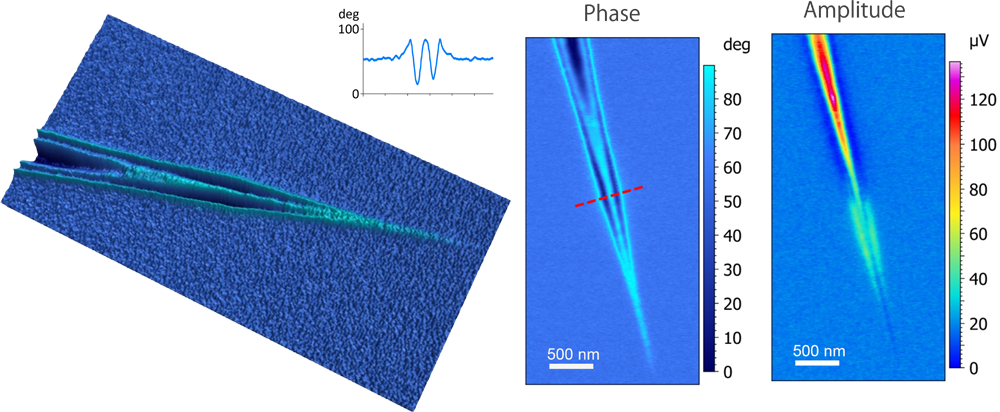
s-SNOM phase and amplitude images of surface plasmon polariton (SPP) on a graphene wedge. (left) 3D view of Phase image. (center) s-SNOM phase with a line cross-section of the SPP standing wave; (right) s-SNOM amplitude.
з”ҹе‘Ҫ科еӯҰ
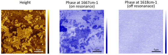
s-SNOM measurements of purple membrane reveal distribution of protein within the lipid membrane. AFM height (top); s-SNOM phase image with IR source tuned to the amide I absorption band (bottom left); s-SNOM phase image off-resonance (bottom right).